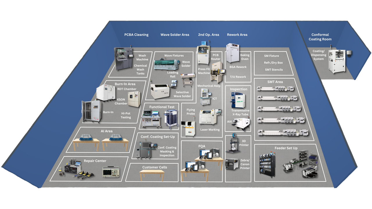
Surface Mount Technology (SMT)
- Purpose: Places surface-mount devices onto a printed circuit board (PCB)
- Key Features: Production floor equipped with 5 SMT Lines, large panel production, low impact placement, dual lane placement, 3D coplanarity check that removes faulty parts
3D Solder Paste Inspection (SPI)
- Purpose: Inspects solder paste deposit quality on PCBs. Detects both catastrophic failures and quality failures in the solder paste deposits.
- Key Features:
- 6,400 mm2/sec inspection speed at 18μm resolution
- Operator can remove a defective PCB from within the machine
- High-precision 0201 pad inspection
Reflow Oven
- Purpose: Melts the solder paste on the PCB to create solder joints.
- Key Features:
- 6 upper and 6 bottom forced hot air convection zones allow high quality lead-free soldering with uniform heating and exceptional process stability
- Temp. accuracy ±1°C and a high-speed CE certificated blower for maximum convection
Automated Optical Inspection (AOI)
- Purpose: Checks for defects in printed circuit board assemblies (PCBAs).
- Key Features:
- Rigid gantry structure and exclusive dual-motor drive system
- High resolution linear scale provides high accuracy positioning
- CoaXPress camera delivers faster inspection and measurement processes
Automated X-Ray Inspection (AXI)
- Purpose: Checks for defects in PCBAs
Key Features:- Fully automatic inspection of hidden solder joints with X-Ray images
- Solder joints inspection in several layers
Transmissive X-Ray Inspection
- Purpose: Displays a real time image of the solder joints that one cannot see by visual inspection
- Key Features:
- 1.33 Mpixel @ 10fps Long
- Lifetime CMOS flat panel detector with real-time image enhancements
- Geometric Magnification 1400X, System 4200X
Flying Probe
- Purpose: Measures each component of a PCB in turn to check that it is in-place and of the correct value
- Key Features:
- Breakthrough 4-heads & 6-flying probes system
- Safe and highly accurate measurement system
- Strong and rigid XY stage
- Key Features:
Baking Oven
- Purpose: Removes moisture from components that are moisture sensitive
Key Features: Can heat items from ambient (room temperature) +25°F to 450°F
Pressfit Machine
- Purpose: Inserts compliant pin connectors into PCBs
Key Features:- Semi-automatic pressing of compliant pins
- Ability to control & monitor force, distance, and speed
RDT Chamber
- Purpose: Tests the effects of specified environmental conditions on electronic devices and components.
- Key Features:
- Temperature range of -80°C to +100°C
- Excellent temperature uniformity
- Multiple cooling circuits and techniques
- Redundant / mission critical design criteria
PCB Router
- Purpose: De-panels PCBs through a router bit that minimizes stress on the components
- Key Features:
- Max cutting speed is 50mm/ sec
- Traveling speed 8000 mm/ sec
- Built-in fixture-based dust vacuum system
- Machine can shift up to 5 depths
Wave Solder
- Purpose: Wets the exposed metallic areas of the board (not protected with solder mask) creating a reliable mechanical and electrical connection.
- Key Features:
- Manual conveyor angle adjustment between 5 to 7 degrees
- Rotary chip wave & lambda
- Temperatures up to 215ºC
- Recipe control single-nozzle spray fluxer
- High-velocity convection topside preheaters
Wash Machine
- Purpose: Washes the PCBAs with DI water (in-line washer) or Chemicals (batch washer)
- Key Features: Built-in process monitoring
3D Printer
- Purpose: Prints 3D models from a CAD file designed by engineering with materials such as ABS, PLA, etc.
- Key Features:
- Allows for a flexible design and rapid prototyping
- Produces strong, light-weight parts while minimizing waste
Conformal Coating
- Purpose: Protects the entire assembled parts or area from moisture, dust, and other harsh conditions
- Key Features:
- Secondary moisture cure mechanism for curing in the non-UV exposed shadowed area
- Fluoresces under UV light to allow for coating inspection
Laser Marking
- Purpose: Marks products that need an identification mark for tracking or recognition.
- Key Features:
- Marks non-metallic surfaces including ceramics, glass, and plastics
- Mark is permanent and consumable costs are low
- Produces a laser cell with a small footprint
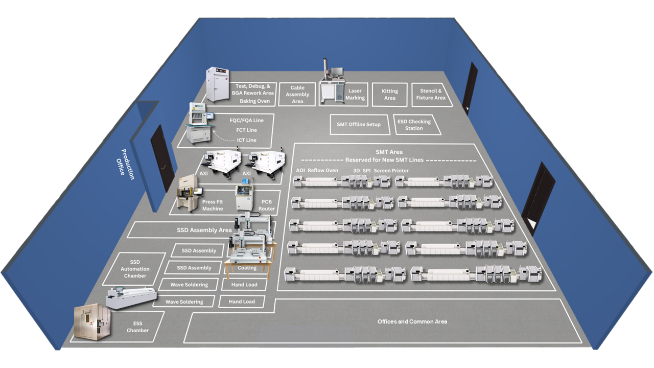
Surface Mount Technology (SMT)
- Purpose: Places surface-mount devices onto a printed circuit board (PCB)
- Key Features:
- Production floor equipped with 12 SMT lines
- Large panel production
- Low impact placement and dual lane placement
- 3D coplanarity check that removes faulty parts, panel warpage check, quick-change feeder carts and nozzle banks
- Lightweight 16-nozzle head with increased placement accuracy
Automated Optical Inspection (AOI)
- Purpose: Test for defects in printed circuit board assemblies (PCBAs)
- Key Features:
- High-speed color multi-angle inspection of up to 01005 components
- High-defect coverage using hybrid 2d+3d inspection technology
- True 3D profile measurement using dual laser units
- Rapid programming interface with auto library and offline editing
Reflow Oven
- Purpose: Used to melt the solder paste on the PCB to create solder joints
- Key Features:
- 8 heating and 2 cooling zones
- Maximum setpoint temperature of 350°C
- Active forced convection top and bottom cooling cells
- Closed-loop convection control
3D Solder Paste Inspection (SPI)
- Purpose: Inspects solder paste deposit quality on PCBs. Detects both catastrophic failures and quality failures in the solder paste deposits.
- Key Features:
- Multi-angle 3D side view
- 5 camera inspection
- Metrology-grade measurements
- SmartWarp compensation eliminates local PCB deformation
- AI-powered algorithms with smart programming
- Industry 4.0 ready platform
Screen Printer
- Purpose: Prints solder paste onto a surface mount assembly forming the PCB with the use of a metal mesh or stencils.
- Key Features:
- 510 x 510mm (optional 650mm long board kit) and auto pin setup for high mix environments
- Print capability to process microchip, to bumping, to pin-in-paste applications
Automated X-Ray Inspection
- Purpose: Test for defects in printed circuit board assemblies (PCBAs)
- Key Features:
- Three-dimensional analysis of solder joints
- Accurate and repeatable measurements with high call accuracy
- Pin-through-pin (PTH) wetting coverage & head-in-pillow (HIP) inspection capability
In-Circuit Test
- Purpose: Measures each component of a PCB in turn to check that it is in-place and of the correct value.
- Key Features:
- Modular upgrade options from Manufacturing Defect Analyzer (MDA) to ICT and functional test
- High fault coverage test solution
- Limited access solution and functional test expansion using PCI Extensions for Instrumentation (PXI) modules
Laser Marking
- Purpose: Marks products that need an identification mark for tracking or recognition.
- Key Features:
- Marks non-metallic surfaces including ceramics, glass, and plastics
- Mark is permanent and consumable costs are low
- Produces a laser cell with a small footprint
Baking Oven
- Purpose: Removes moisture from components that are moisture sensitive
- Key Features:
- Bi-metal thermostat
- Temperature accuracy of ±3°C
- Temperature is controlled by PID digital microprocessor, gravity convection (GCE), or Air Forced (AFE)
Press Fit Machine
- Purpose: Inserts compliant pin connectors into PCBs
- Key Features:
- Semi-automatic pressing of compliant pins
- Ability to control & monitor force, distance, and speed
PCB Router
- Purpose: De-panels PCBs through a router bit that minimizes stress on the components
- Key Features:
- Max cutting speed is 50mm/ sec
- Traveling speed 8000 mm/ sec
- Built-in fixture-based dust vacuum system
- Machine can shift up to 5 depths
Environmental Stress Screening (ESS) Room
- Purpose: Tests the effects of specified environmental conditions on electronic devices and components.
- Key Features:
- Excellent temperature uniformity
- Multiple cooling circuits and techniques
- Redundant / mission critical design criteria
- All major subsystems procured from world class manufacturers